
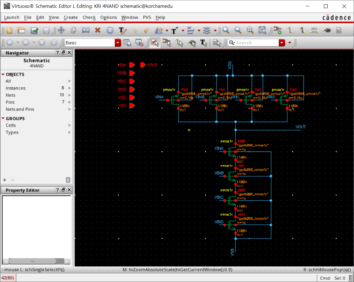
1. 4NAND GATE
1) circuit schematic
2) test (width 찾기)
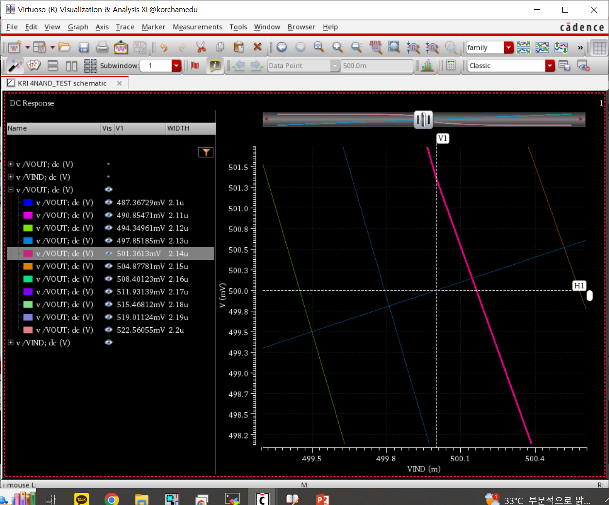
nmos width 1u일때 기준 pmos width = 2.14um로 결정
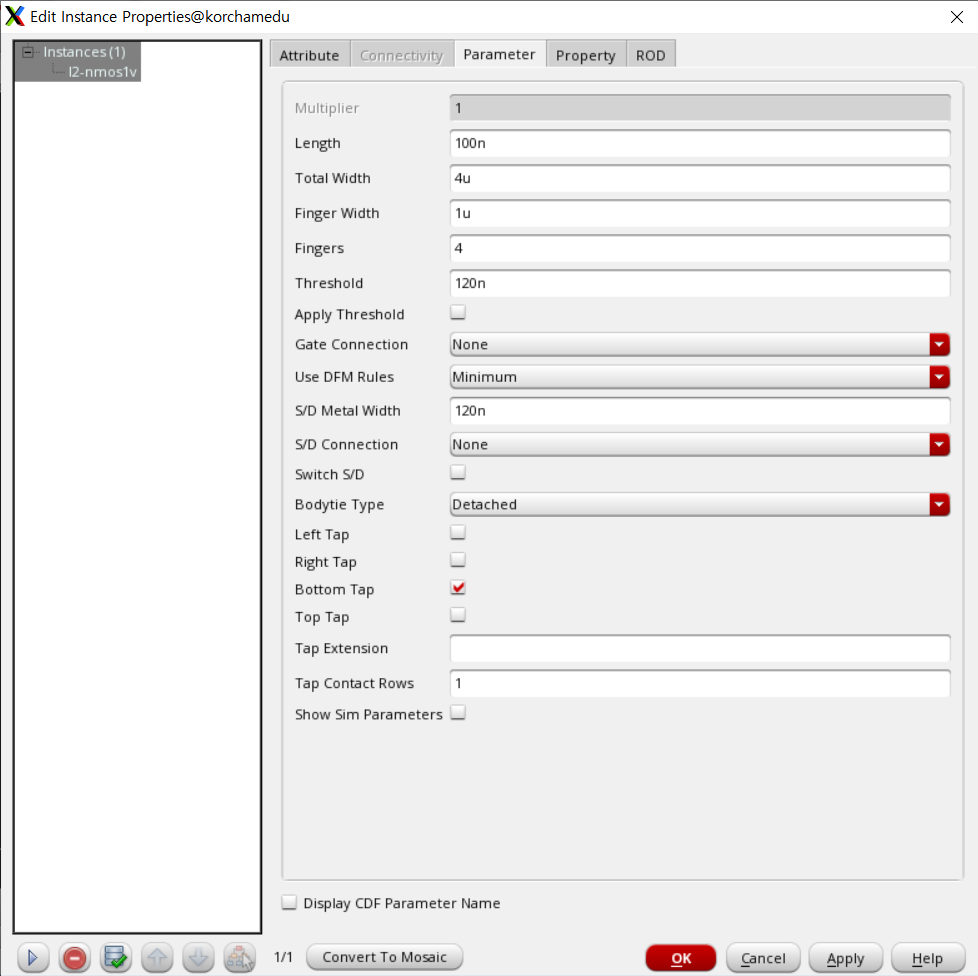
3) layout schematic
- finger setting

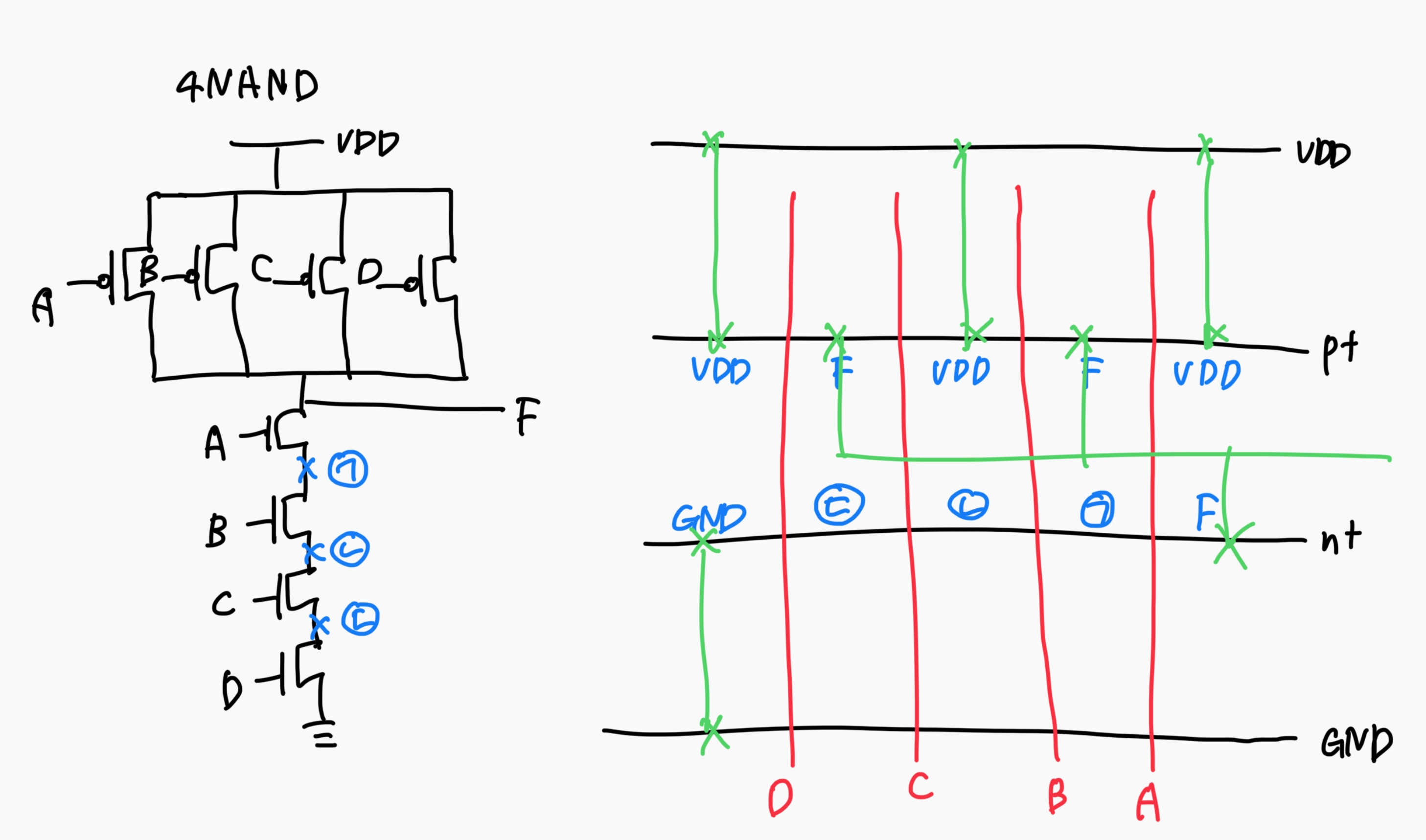
- circuit schematic & stick diagram
- schematic
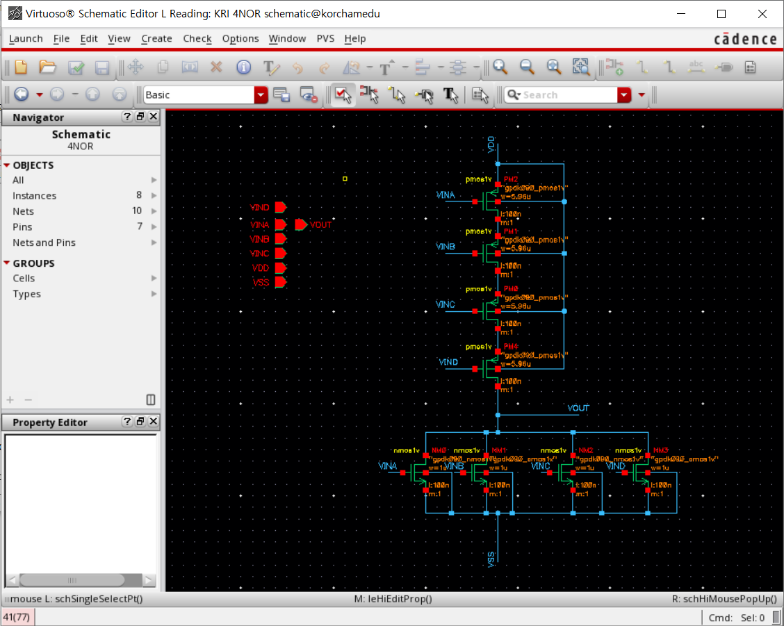
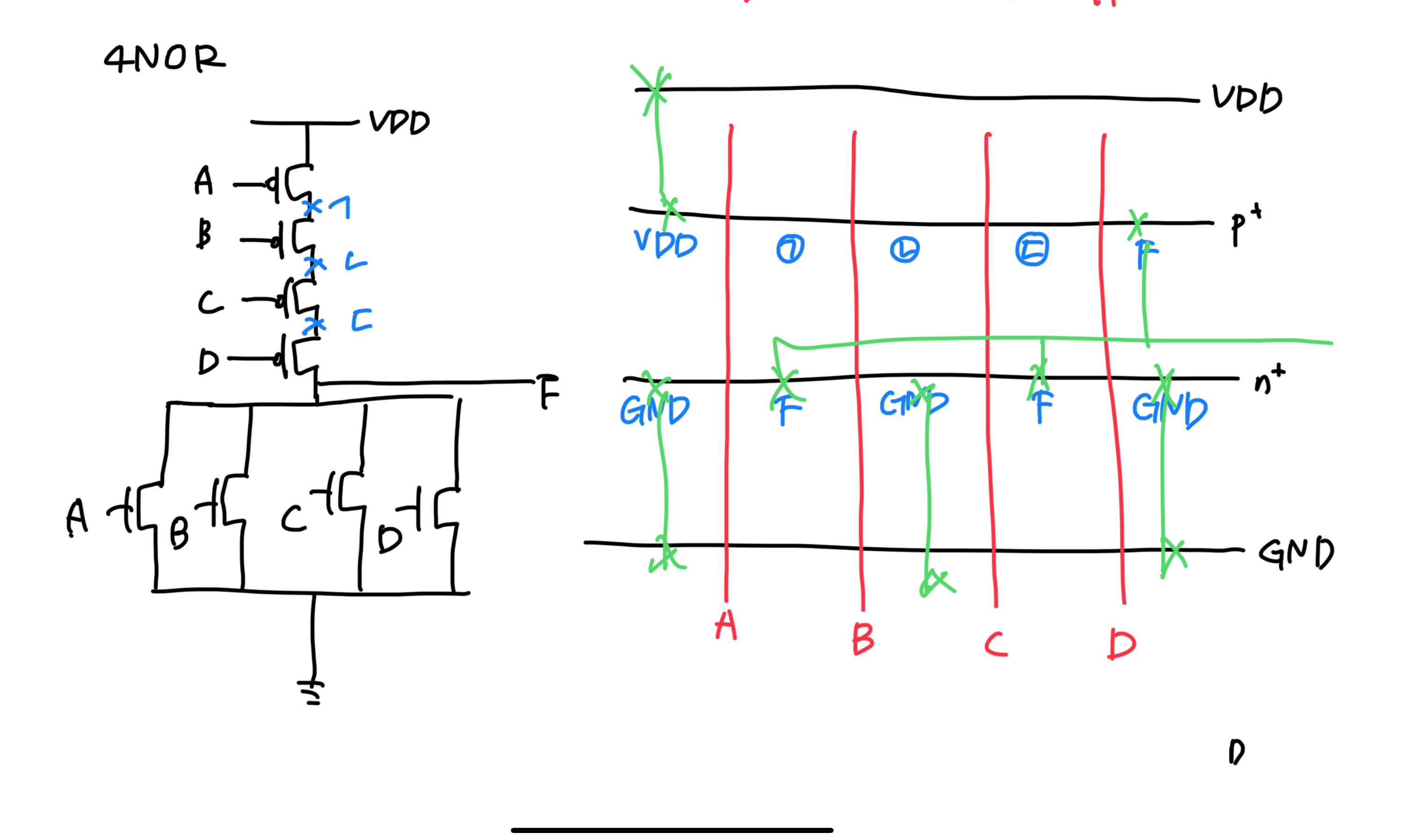
2. 4-input NOR Gate
1) circuit schematic
2) test simulation (find pmos width)
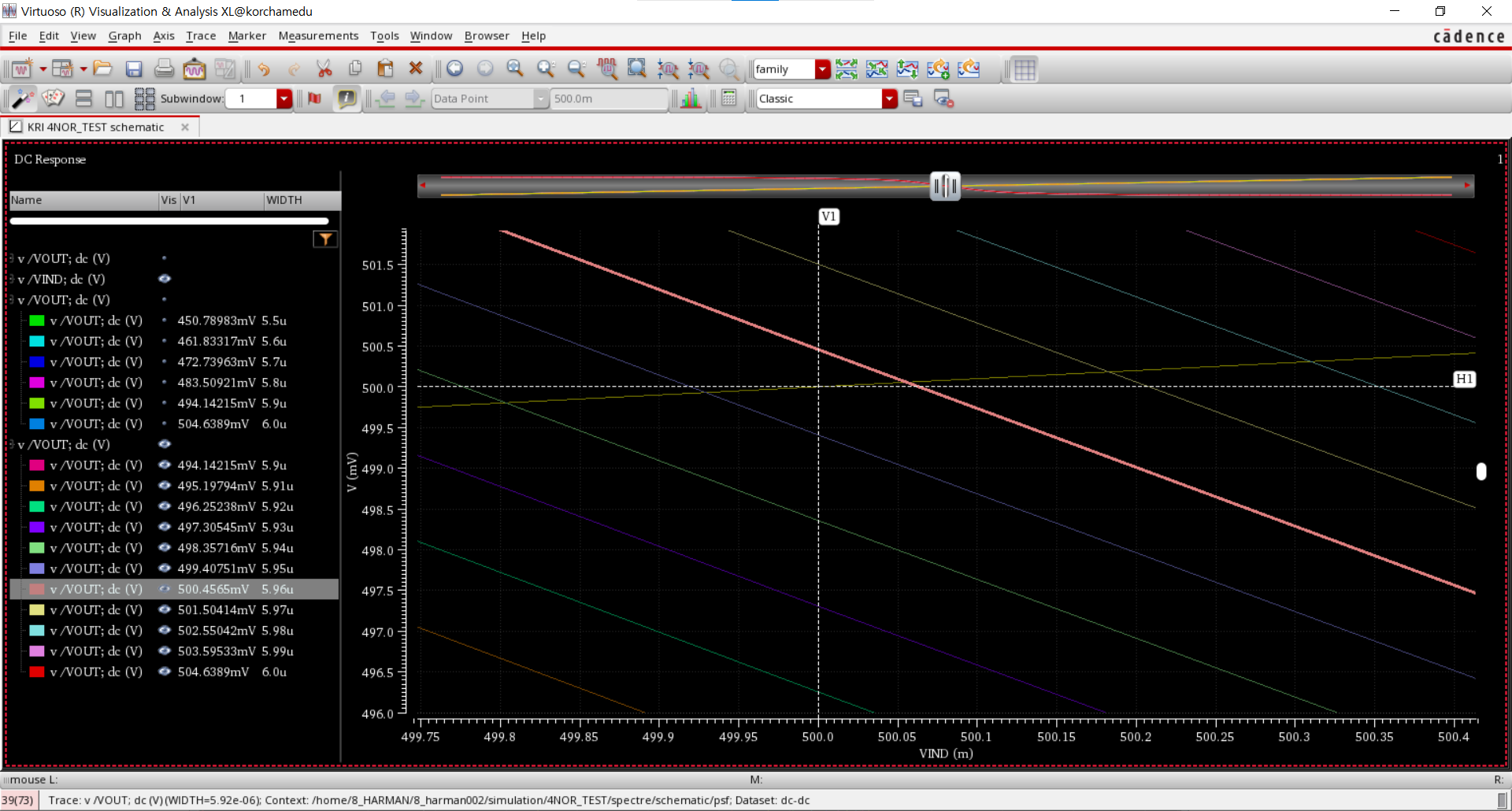
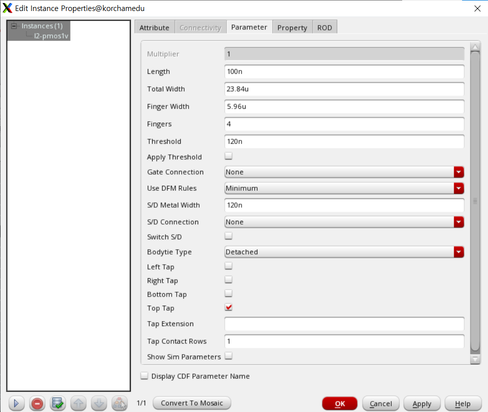
pmos width = 5.96um일때 조건 충족
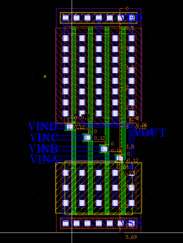
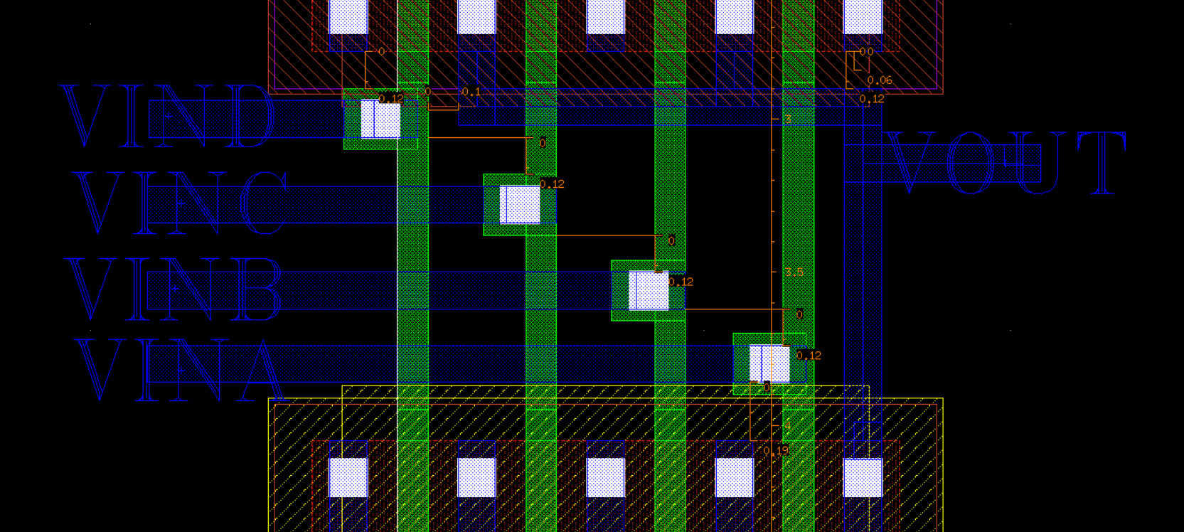
3) layout schematic
- finger setting

- circuit schematic & stick diagram
- shcematic
'하만 세미콘 아카데미 8기 > Full Custom One Chip 설계' 카테고리의 다른 글
| Full Custom One Chip Design potfolio (0) | 2024.09.01 |
|---|---|
| 240812 2 to 1 MUX Layout 설계 - nand & not inv / switch 이용 (0) | 2024.08.19 |
| 240809 - 2 NOR / 3 NOR Gate layout 설계 (0) | 2024.08.09 |
| 240808 2NAND Gate / 3NAND Gate layout 설계 (0) | 2024.08.08 |
| 240807 - 3 input NAND gate / 3 input NOR GATE (0) | 2024.08.07 |
1. 4NAND GATE
1) circuit schematic
2) test (width 찾기)
nmos width 1u일때 기준 pmos width = 2.14um로 결정
3) layout schematic
- finger setting
- circuit schematic & stick diagram
- schematic
2. 4-input NOR Gate
1) circuit schematic
2) test simulation (find pmos width)
pmos width = 5.96um일때 조건 충족
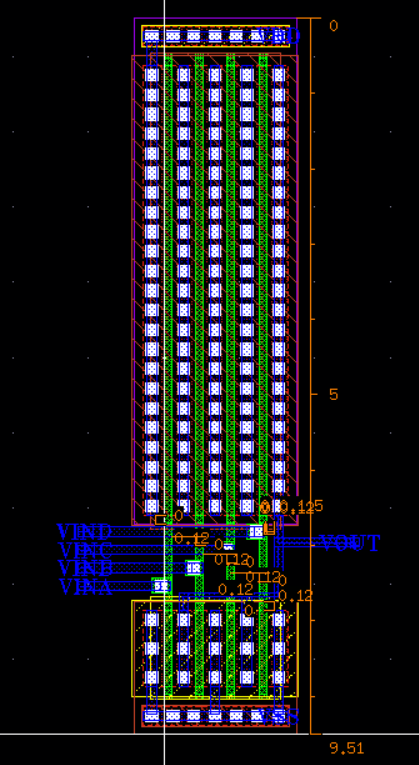
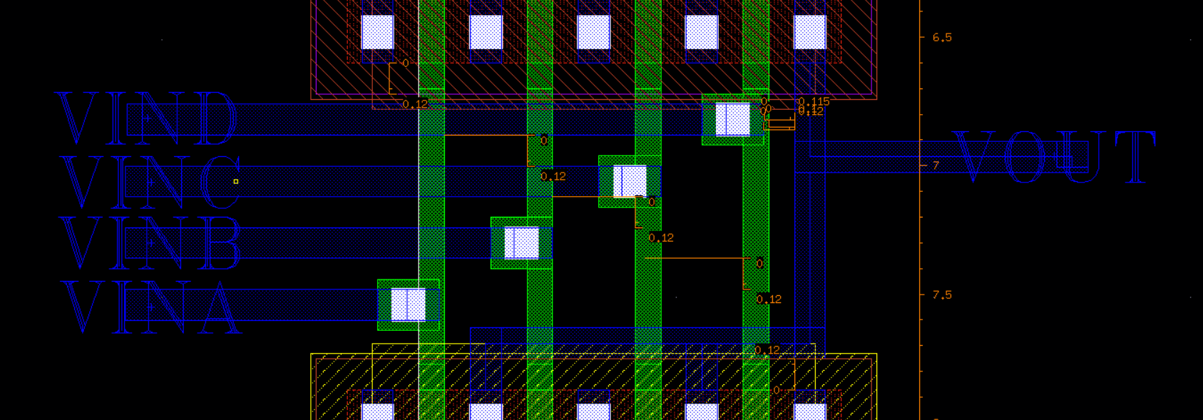
3) layout schematic
- finger setting
- circuit schematic & stick diagram
- shcematic
'하만 세미콘 아카데미 8기 > Full Custom One Chip 설계' 카테고리의 다른 글
| Full Custom One Chip Design potfolio (0) | 2024.09.01 |
|---|---|
| 240812 2 to 1 MUX Layout 설계 - nand & not inv / switch 이용 (0) | 2024.08.19 |
| 240809 - 2 NOR / 3 NOR Gate layout 설계 (0) | 2024.08.09 |
| 240808 2NAND Gate / 3NAND Gate layout 설계 (0) | 2024.08.08 |
| 240807 - 3 input NAND gate / 3 input NOR GATE (0) | 2024.08.07 |