
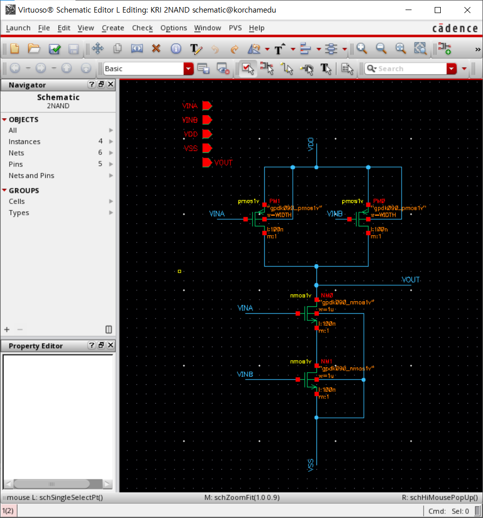
1. 2NAND schematic
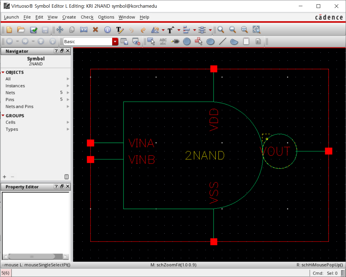
2. symbol
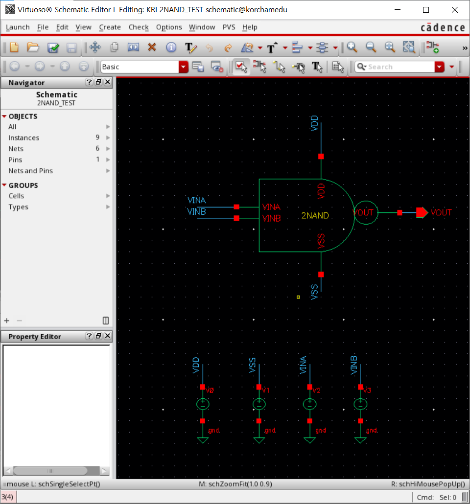
3. test schematic
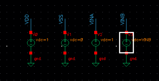
4. simulation
- 전압값 설정 (단축키 'Q')
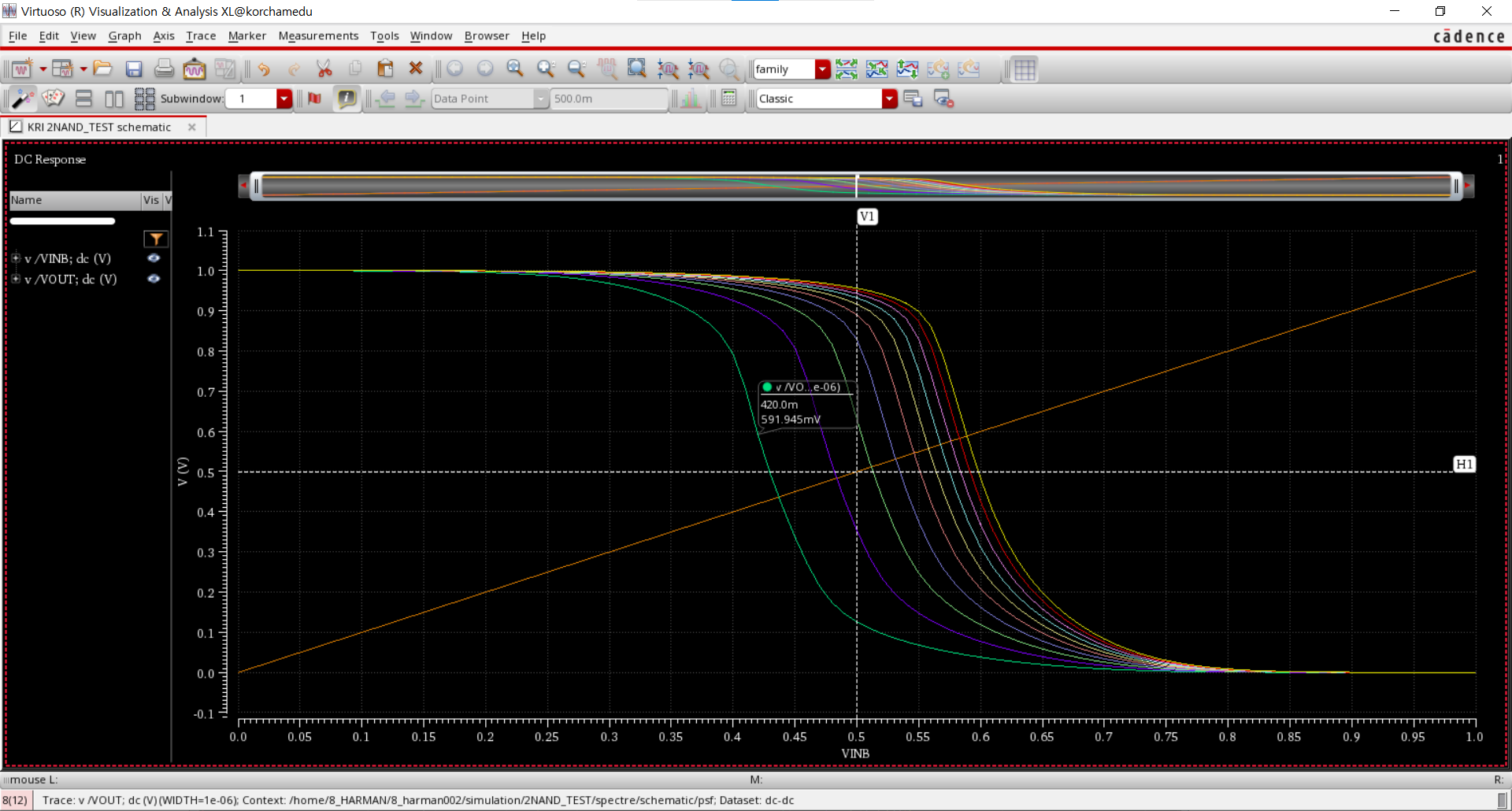
- result plot
- width : 1u~10u 범위 내 simulation result
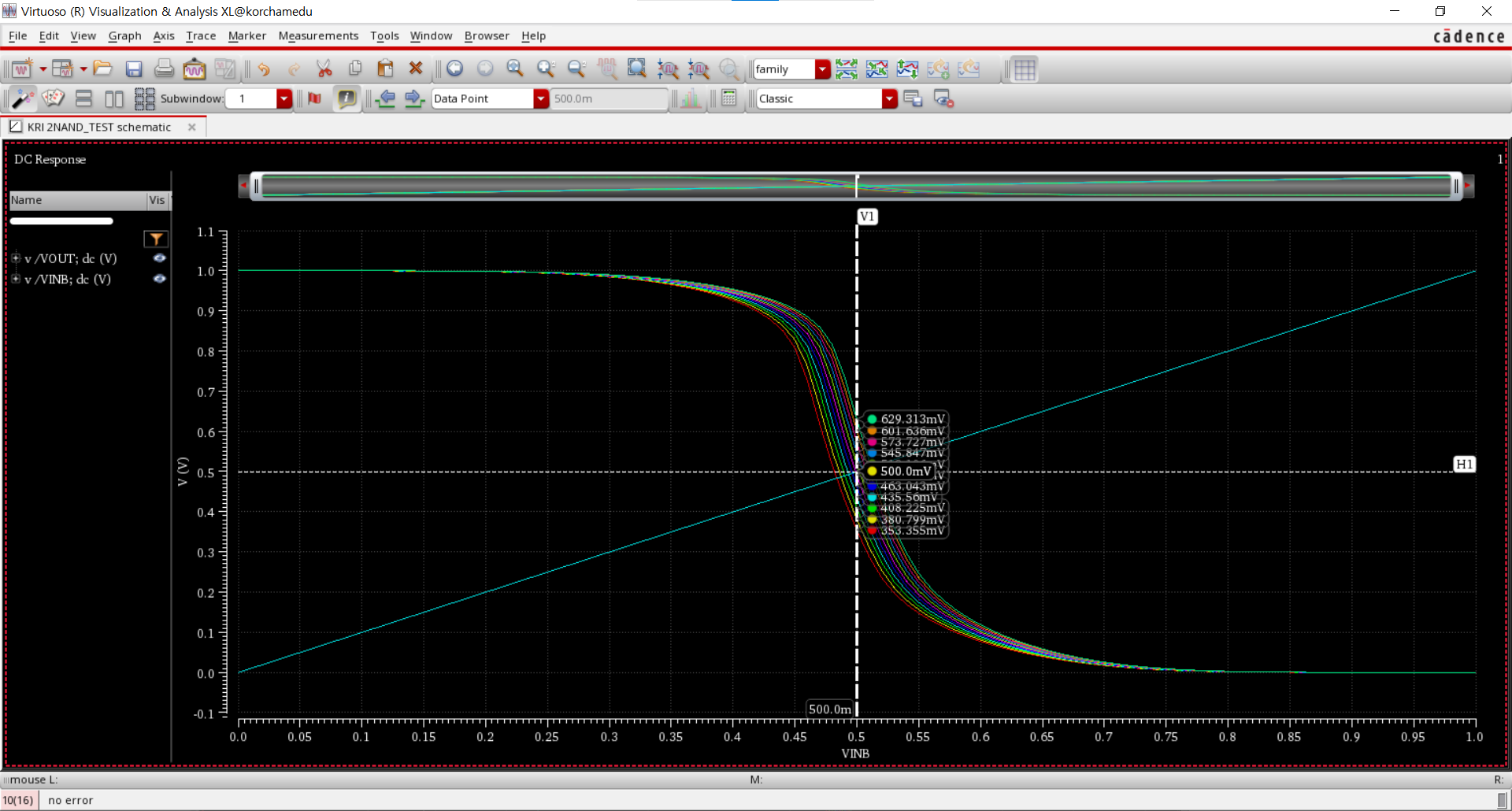
- width : 2u~3u 범위 내에서의 simulation
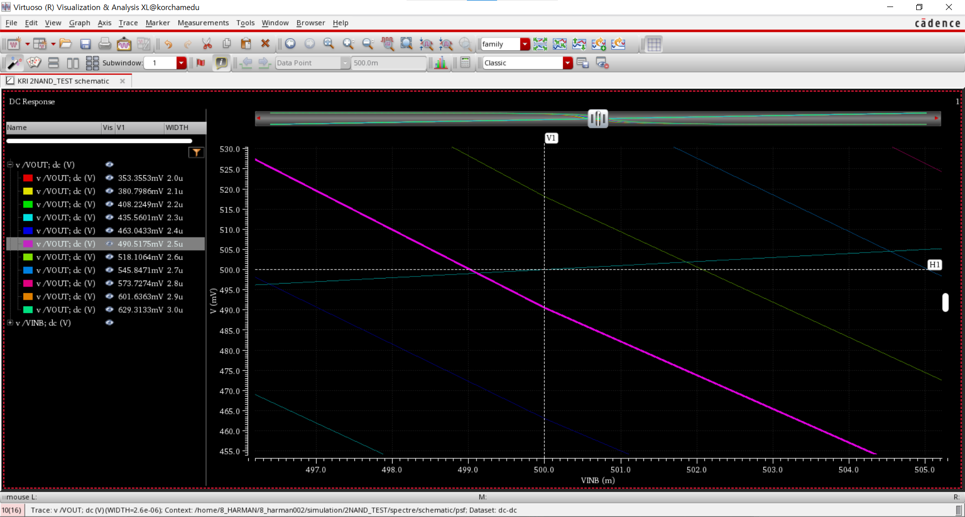
-> 2.5u~2.6u 범위 내에서 다시 go
- width : 2.5u~2.6u
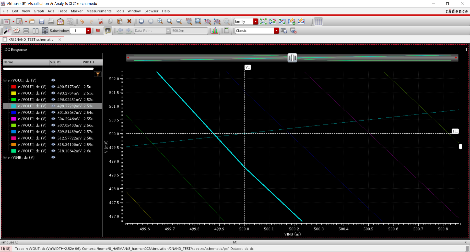
2.53um일때 Vin = 500mV와 가장 근접한 결과 얻을 수 있다
-> width = 2.53um로 결정
'하만 세미콘 아카데미 8기 > Full Custom One Chip 설계' 카테고리의 다른 글
| 240807 - 3 input NAND gate / 3 input NOR GATE (0) | 2024.08.07 |
|---|---|
| 240807 - 2NOR 실습 (0) | 2024.08.07 |
| 240806 실습 - inverter (0) | 2024.08.06 |
| 240806 (0) | 2024.08.06 |
| mobaXterm - virtuoso 실행 (0) | 2024.08.05 |
1. 2NAND schematic
2. symbol
3. test schematic
4. simulation
- 전압값 설정 (단축키 'Q')
- result plot
- width : 1u~10u 범위 내 simulation result
- width : 2u~3u 범위 내에서의 simulation
-> 2.5u~2.6u 범위 내에서 다시 go
- width : 2.5u~2.6u
2.53um일때 Vin = 500mV와 가장 근접한 결과 얻을 수 있다
-> width = 2.53um로 결정
'하만 세미콘 아카데미 8기 > Full Custom One Chip 설계' 카테고리의 다른 글
| 240807 - 3 input NAND gate / 3 input NOR GATE (0) | 2024.08.07 |
|---|---|
| 240807 - 2NOR 실습 (0) | 2024.08.07 |
| 240806 실습 - inverter (0) | 2024.08.06 |
| 240806 (0) | 2024.08.06 |
| mobaXterm - virtuoso 실행 (0) | 2024.08.05 |